B02 group
B02-1 Assessment and control of radiative recombination mechanisms in singularity structures by scanning near-field optical microscopy
- Principal Investigator / Yoichi Kawakami (Kyoto University / Professor)
- Co-Investigator / Mitsuru Funato (Kyoto University / Associate Professor)
- Co-Investigator / Ryota Ishii (Kyoto University / Assistant Professor)
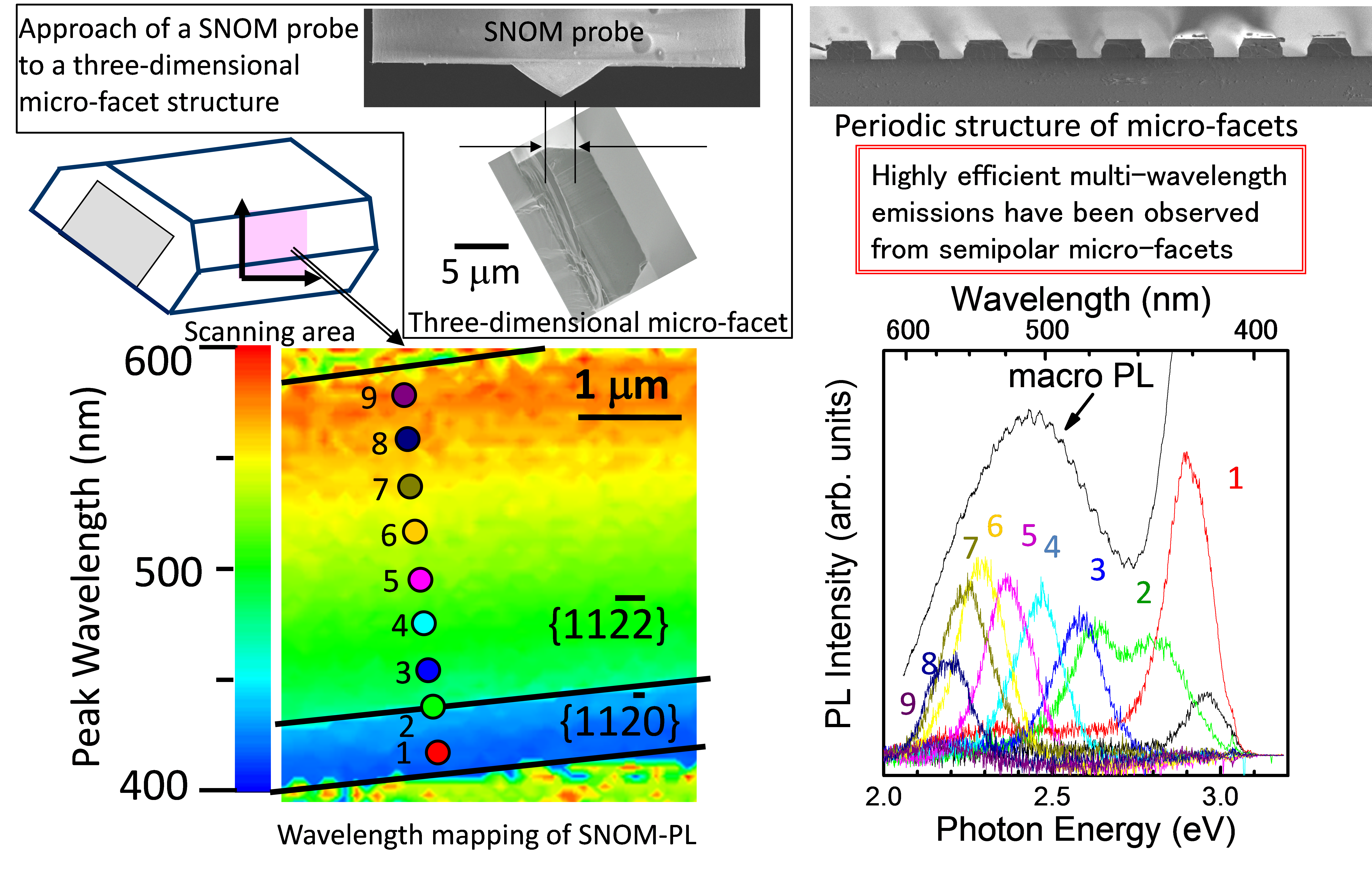
We strive to clarify the design concept of light emitting devices with the ultimate goal of achieving 100% internal quantum efficiency in the full visible spectrum by focusing on singularity structures such as semipolar micofacets and nanocolumns in (Al,Ga,In)N-based three-dimensional semiconductors. To assess InGaN-based nanostructures and elucidate the mechanism of radiative recombination in singularity structures by visualization of exciton and carrier motions, we employ original laboratory-made SNOM (scanning near-field optical microscopy) systems, including DSNOM (dual-probe SNOM). Moreover, we plan to establish a near-field technique in the DUV (deep ultraviolet) spectra by developing an optical probe material capable of guiding DUV light with a highly efficient transmittance. These efforts should lead to the study of spatially and temporally resolved recombination dynamics in AlGaN-based and InGaN-based nanostructures. Furthermore, we focus on the effect of plasmonics, where the controllability of the emission wavelength and the key for high emission efficiency will be characterized in compositionally modulated singularity structures. These studies should help realize next-generation devices such as phosphor-free tailor-made lighting and highly efficient DUV emitters due to the clear design concept of singularity structures intended to control the optical functionalities.
B02-2 Studies on the local luminescence dynamics in singularity structures by using spatio-time-resolved cathodoluminescence technique
- Principal Investigator / Shigefusa F. Chichibu (Tohoku University / Professor)
- Co-Investigator / Kazunobu Kojima (Tohoku University / Associate Professor)
- Co-Investigator / Kohei Shima (Tohoku University / Assistant Professor)
- Co-Investigator / Taizo Nakasu (Tohoku University / Assistant Professor)
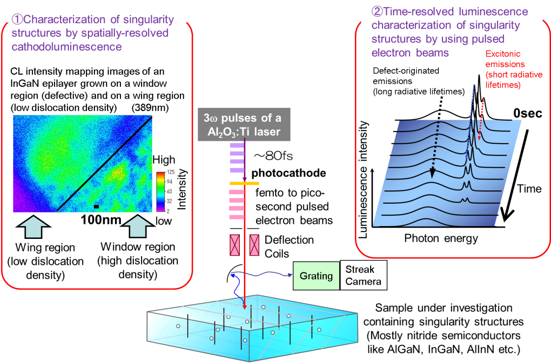
Singularity structures including imperfections as well as inhomogeneity contain various types of heterointerfaces within the bulk and/or surfaces. For understanding local carrier and/or emission dynamics in such structures, probing local emission dynamics by using a method that picks off them is mandatory. Our principal task in this singularity project is obtaining the images of multiple mapping of luminescence intensity, energy, and lifetime by using our unique 'Spatio-Time-Resolved Cathodoluminescence (STRCL)' system. This system is basically composed of a cathodoluminescence (CL) measurement system equipped on a scanning electron microscopy (SEM), but its electron beam (e-beam) gun is replaced by a pulsed photoelectron (PE) gun made of Au, which is excited using the frequency-tripled femtosecond pulses of mode-locked Al2O3:Ti laser. Because e-beam pulses are used as an excitation source, STRCL has principally no limitation on the bandgap energy of a material to be measured. We will collaborate with all groups to assess the carrier recombination dynamics and quantum effects in the singularity structures for creating new optoelectronic sciences in semiconductors.
B02-3 Optical properties and functionalities of dense excitonic systems in singularity structures
- Principal Investigator / Yoichi Yamada (Yamaguchi University / Professor)
- Co-Investigator / Satoshi Kurai (Yamaguchi University / Assistant Professor)
We maintain a particular focus on the many-body effects of excitons in nitride semiconductors. Owing to the advantages of excitonic nature that are large exciton binding energy and strong oscillator strength, the excitons stably exist at high excitation densities, where the interaction between two or more excitons causes the unique properties that are characterized by the formation of biexcitons and the inelastic scattering of excitons. From the viewpoint of excitonics (exciton engineering), it is important to study the recombination dynamics of dense excitonic phenomena because the contribution of excitonic processes to optical transitions is expected to improve the performance of semiconductor optoelectronic devices, such as light-emitting diodes and laser diodes. The singularity structure we study mainly in the present work is an inhomogeneous system caused by structural imperfection such as alloy fluctuations and quantum-size fluctuations. We study the effect of localization as well as dimensionality on dense excitonic systems by means of a variety of laser spectroscopy: selective and resonant excitation spectroscopy using a wavelength-tunable dye laser, time-resolved spectroscopy using a femtosecond titanium sapphire laser, and space-resolved spectroscopy using a cathodoluminescence mapping system combined with scanning electron microscopy. We clarify the potential of the singularity structure and obtain a guide to the design of high-efficiency excitonic optoelectronic devices.
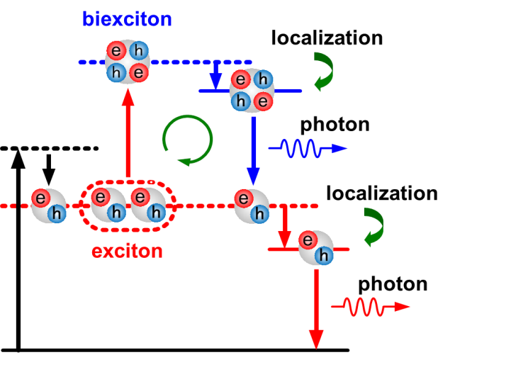
Localization and radiative recombination of excitons and biexcitons in an inhomogeneous system
B02-19-1 Theoretical modeling of electronic structures in III-nitride materials with singular structures based on photo-acoustic and photoluminescence simultaneous measurements
- Principal Investigator / Atsushi A. Yamaguchi (Kanazawa Institute of Technology / Professor)
III-nitride based optical devices such as light-emitting diodes and laser diodes have been already commercialized. However, their active-layer materials, alloy semiconductor InGaN and AlGaN, have singular structures such as alloy compositional fluctuation, spatial strain distribution, and various defects, and their optical properties have not been fully understood. Studies on radiative and nonradiative recombination mechanisms are very important to clarify the electronic structures and carrier dynamics in the III-nitride semiconductors with singular structures. In this study, we will directly observe both the two carrier recombination processes under the same optical excitation condition by photo-acoustic and photoluminescence simultaneous measurements, which we have newly developed, and we will estimate the internal quantum efficiency in the singular structures. Lifetimes of both the radiative and nonradiative recombination processes will be obtained by the combination with photoluminescence decay time measured by time-resolved photoluminescence spectroscopy. Furthermore, we will try to propose a theoretical model to reproduce all the reported experimental results to comprehensively understand the electronic structures and carrier dynamics in the singular structures.
Page topB02-19-2 Theory of migration and deformation of singularity structures via electron-phonon interaction
- Principal Investigator / Masato Oda (Wakayama University / Lecturer)
Nitride based semiconductors are the most important materials for light-emitting devices and are also expected as candidates for next-generation power devices. However, while application research is promoted, there remain unsolved problem that device degradation is caused by migration and deformation of singularity structures such as dislocations. In this study, we aim to clarify the microscopic mechanism in which the singularity structure migrates and deforms by focusing on the electron-phonon interaction, and to find its control method. If the migration and deformation of the singularity structure can be controlled, it can be expected that the device life will be extended and leading to a technology to create a structure with new functions.
Page topB02-19-3 Fabrication of plasmonic nanostructures using InGaN nanocolumns with singular lattice arrays and their optical functionality control
- Principal Investigator / Takao Oto (Yamagata University / Assistant Professor)
Emission efficiencies in InGaN based light emitting diodes (LEDs) dramatically decreases with increasing emission wavelength. To realize next-generation full-color optical device applications such as micro-LED displays, the green to red LED performance should be improved. In this study, we will improve the emission efficiencies for the green and red regions by introducing metal/dielectric hybrid periodic nanostructures "plasmonic crystals" based on columnar nanocrystals "nanocolumns (nanowires)" with singular lattice arrays to InGaN based light emitters. In the nanocolumn plasmonic crystals, the light emission enhancement due to the surface plasmon coupling is simultaneously obtained in addition to the photonic crystal effect and the nanostructural effects such as dislocation-free nature, strain relaxation, and high light extraction. Therefore, the significant improvement of emission efficiencies is highly promising. Moreover, by investigating the influence of singular lattice array on the optical and plasmonic characterizations in InGaN in detail, we will attempt to develop the optical devices with novel optical functionalities which cannot be theoretically realized by using conventional triangular lattices.
Page topB02-19-4 Specific surface nanostructures and optical control of plasmonic metamaterials based on oxide semiconductors
- Principal Investigator / Hiroaki Matsui (The University of Tokyo / Associate Professor)
We focus on specific surface nanostructures self-formed during film growth of zinc oxide (ZnO) in II-IV semiconductors. In the conventional film growth, two-dimensional surfaces (perfect surfaces) based on layer-by-layer and step-flow modes have played an important role in controlling structural interfaces between similar and dissimilar materials in the fields of film growth related to quantum-well and super-lattice structures. In this study, we introduce the specific surface nanostructures (imperfect surfaces) in an effort to control plasmonic properties of hyperbolic metamaterials on ZnO (ZnO-HMMs). In particular, we aim at clearing growth mechanism and its control of the specific surface nanostructures including structural defects for optical applications in the near-infrared applications.
Page topB02-19-5 Nanoscale control and in-situ characterization of singularity structures in single-layered semiconductors using tip-enhanced near-field optical techniques
- Principal Investigator / Taka-aki Yano (Tokyo Institute of Technology / Assistant Professor)
Tip-enhanced optical spectroscopy, a family of scanning probe microscopy techniques, has been recognized as a near-field optical technique. A sharp metallic tip is utilized to plasmonically confine and enhance the incident light at the tip apex. In this work, we propose to utilize the metallic probe tip not only to locally excite Raman scattering and photoluminescence from single-layered semiconductors, but also to locally apply external stimuli to the sample surface through the tip apex. The tip-applied stimuli including pressure and voltage are likely to induce singularity structures (lattice distortion, defects etc.) in single-layered semiconductors in the vicinity of the tip apex. Combination of tip-enhanced optical spectroscopy with the local external stimuli has now opened up a new way to control the singularity structures on a nanometer scale along with the in situ nano-analysis, which can contribute to active functional control of nanodevices.
Page topB02-19-6 Development of functionality in protonic-defect induced organic crystals by photon irradiation
- Principal Investigator / Yuka Kobayashi (National Institute for Materials Science / Principal Researcher)
Protonic defects induce electroactive properties in organic crystals. An effect of photon irradiation to the protonic-defect induced crystals is investigated in order to develop variety of electronic properties.
Page top