A02 group
A02-1 Development of diamond electron device using III-nitride nanolaminate singularity structure
- Principal Investigator / Yasuo Koide (National Institute for Materials Science / Executive Vice President)
- Co-Investigator / Masataka Imura (National Institute for Materials Science / Senior Researcher)
- Co-Investigator / Meiyong Liao (National Institute for Materials Science / Senior Researcher)
- Co-Investigator / Jiangwei Liu (National Institute for Materials Science / Independent Researcher)
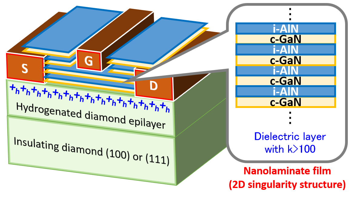
Recently, a nanoscale multilayer material using Al2O3/TiO2, named by nanolaminate layer, has been reported to provide a high dielectric constant (k) larger than 1000 due to dielectric relaxation by Maxwell-Wagner effect. The purpose of this research is twofold. The first is to develop a singularity structure of the nanolaminate layer composed of dielectric i-AlN and conductive c-GaN with k larger than 100 and the respective 1 nm thickness. The second is to demonstrate a new-concept diamond transistor using this nanolaminate layer gate on hydrogenated (H) diamond surface. The hole carrier density in the H-terminated diamond surface is reported by our research group to be as large as 1014 cm-3 which is one-order of magnitude larger than that of commercialized AlGaN/GaN heterojuntion transistor. In order to control such the high-density hole carrier, it is required to develop the gate insulator with k larger than 100. The development of the AlN/GaN nanolaminate singularity structure is a key to success.
A02-2 Research on novel light emitting devices by using the properties of singularity structure crystals
- Principal Investigator / Hideki Hirayama (RIKEN / Chief Scientist)
- Co-Investigator / Wataru Terashima (RIKEN / Researcher)
- Co-Investigator / Norihiko Kamata (Saitama University / Professor)
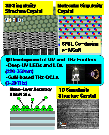
In this work, we explore novel light emitting devices by introducing and using the properties of singularity structure crystals. In order to realize unexplored deep-ultraviolet (DUV) and terahertz (THz) light emitting devices, it is necessary to achieve a high hole concentration p-type AlGaN, a low dislocation density AlN buffer layer as well as AlGaN multi-stacking superlattices (SLs) with atomically flat hetero-interfaces. In this project, we will realize more than 50 % efficiency DUV light-emitting diodes (LEDs) and laser diodes (LDs) by developing pillar AlN array light extraction structure by using a self-assembling growth method and/or by developing high hole concentration p-AlGaN layers with co-doping in short-period superlattices (SPSLs). In order to achieve quantum-cascade lasers (QCLs), we need AlGaN/GaN multi-stacking SL structures with atomically flat hetero-interfaces. We will realize unexplored frequency THz-QCLs by developing high optical gain multi-stacking AlGaN/GaN high-quality SLs by using our original droplet elimination by thermal annealing (DEAT) growth method.
A02-3 Characterization and control of GaN heterointerfaces including singularity structures for advanced electron devices
- Principal Investigator / Tamotsu Hashizume (Hokkaido University / Professor)
- Co-Investigator / Masamichi Akazawa (Hokkaido University / Associate Professor)
- Co-Investigator / Taketomo Sato (Hokkaido University / Associate Professor)
GaN-based heterosystems utilizing various kinds of singularity structures and potential barriers will be high-level heterointerface continuum applicable to next-generation optical and electron devices. On the other hand, such hterointerfaces generally include high-density electronic states causing deterioration of device performances. To apply heterosystems utilizing singularity structures to high-performance devices, it is inevitable to characterize and control of interface electronic states in the vicinity of singularity structures.
In this project, we will precisely characterize electronic states of GaN-based heterosystems including singularity structures by a rigorous simulation of capacitance-voltage characteristics, transient capacitance methods and admittance analyses. From comparative studies between structural/chemical properties and electronic states, in addition, control schemes and/or processes for electronic states will be achieved.
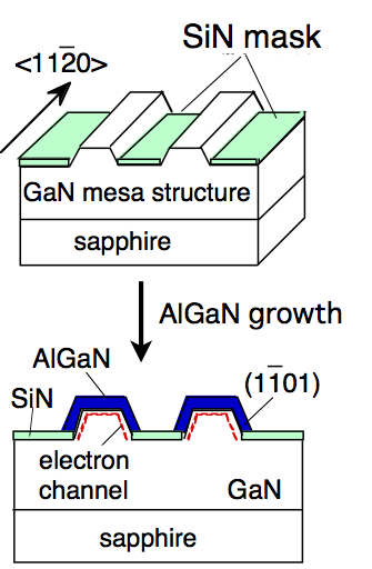
For development of a novel electron device, we will fabricate a multi nanostructure having sidewall channels on a non-polar or a semi-polar GaN surface, as shown in the figure. In addition, we will develop novel sensor devices and ultralow resistance electrodes on the basis of nano-porous GaN structures prepared by an electrochemical process.
A02-19-1 Study on vertical FETs utilizing GaN-based singularity structures and its characterization technology for their performance improvement
- Principal Investigator/ Junichi Motohisa (Hokkaido University / Professor)
GaN-based FETs are attracting interest as next-generation power devices, and one of the interests is focused on the vertical FETs in combination with multiple-gate and nanoscale structures. Our main objectives in this research are to realize vertical multiple-gate FETs based on GaN-based singular structures, namely, GaN nanowires. Towards this goal, we develop technologies to realize GaN nanowires suitable for vertical FETs by selective epitaxy or by nanofabrication technique, and device processing technology to realize vertical FETs. At the same time, towards performance improvement of FETs and devices application of singular structures, we will develop a technology to perform electrical characterization of individual singular structures , for example, by forming nano-scale electrodes in each singular structures by electrochemical process, on which conductive tip of atomic-force microscope is loaded to measure their current-voltage characteristics.
Page topA02-19-2 Functions and applications of freedom of space and disordered states existing in crystals
- Principal Investigator / Katsumi Tanigaki (Tohoku University / Professor)
We are planning to make exploratory researches for the following two important items in terms of the freedom in space and the disordered states existing in single crystals: One being the unification of anharmonic phonons created in materials with having large freedom of space in single crystals and the other being the disordered states existing on the surface or the grain boundaries in crystals. Anharmonic phonons in the former generate good thermoelectrics and disordered states in the latter will lead to good ambipolar carrier injection for highly-efficient light-emitting diodes towards electrically driven lasers
Page topA02-19-3 Physical properties of multilayer graphene emerging from singularity in turbostratic structures
- Principal Investigator / Yoshihiro Kobayashi (Osaka University / Professor)
Graphene has unique and practically useful physical properties, which are evident only for monolayer graphene and should be degraded for multilayer graphene due to strong interaction between graphitic layers. In this research, we will investigate multilayer graphene with singularity structure of turbostratic stacking. Turbostratic structure disturbs crystallographic periodicity for stacking direction and is commonly regarded as "defect" in graphite crystal with regular Bernal stacking. We utilize the turbostratic structure to reduce the interaction between the layers, resulting in emergence of quasi monolayer properties from multilayer graphene. We will develop novel processes to synthesize multilayer turbostratic graphene. As the first approach, defective graphene oxide (GO) is heated at ultrahigh temperature around 1800 °C under reactive environment including alcohol. Defects in the GO induced during chemical exfoliation of graphite should be repaired simultaneously by the thermal process. Turbostratic graphene film is also synthesized by overlayer growth on a template monolayer graphene by CVD process. We expect the turbostratic structure dramatically improve electrical/thermal properties of multilayer graphene. Scalable production of high-performance graphene developed by this study will stimulate practical application of graphene to various fields not restricted to conventional ones.
Page topA02-19-4 Development of fabrication method for novel random lasers based on laser processing technique
- Principal Investigator / Hideki Fujiwara (Hokkai-Gakuen University / Professor)
A random laser operated by a feedback mechanism based on multiple light scattering can simultaneously realize low spatial coherence like a thermal light source and high emission intensity like a laser. Therefore, it has attracted attention as a speckle-free and intense light source for full field imaging and sensors. However, conventional random lasers have problems such as high threshold operation, difficulty in lasing mode control, and limited lasing wavelength band (from UV to visible region). In this work, the aim is the development of a novel laser processing technique to fabricate a new type of random lasers. Using a laser processing technique, I attempt to improve the crystallinity of a materials as well as a macroscopic feedback structure by controlling the laser processing and environmental conditions.
Page topA02-19-5 Thienoisoindigo based single crystal transistors responding to near-infrared light
- Principal Investigator / Minoru Ashizawa (Tokyo Institute of Technology / Assistant Professor)
Organic materials absorbing near-infrared light are very attractive for the fabrication of optoelectronic devices. Especially, near-infrared light has high transparency to biological tissues, thus effective utilization technologies of this energy region are highly in demand. In view of organic field effect transistors (OFETs), multi-functional properties are required in addition to the conventional switching function. In this study, we aim to develop OFETs responding to near-infrared light though incorporation of specific structures into the crystalline thin film. The developed thienoisoindigo (TII) molecules are composed of oligomeric or polymeric TII units absorbing near-infrared wavelength and alkylsilyl acetylene spacers forming specific structures in the crystalline thin film. When the crystalline thin film is exposed to a near-infrared laser, the surface temperature exhibits steep increase through photo-thermal conversion. The generated heat induces free-rotation of alkylsilyl acetylene spacers, leading to formation of disordered structures in the thin film. The OFETs can directly detect structural change associated with specific structure formation as changing transistor parameters.
Page topA02-19-6 Development of high-performance terahertz functional devices utilizing crystal imperfections
- Principal Investigator / Yukio Kawano (Tokyo Institute of Technology / Associate Professor)
Although impurities, lattice defects, etc., are generally regarded as causes of imperfections for high quality semiconductors, most of their corresponding dynamics belong to the terahertz (THz) frequency band. Electronic materials with imperfections are thus expected to be used as novel THz devices by utilizing features such as strong coupling with electromagnetic waves and high responsivity to external fields. However, there was almost no attempt for their active applications to THz devices. This research is aimed at the development of THz functional devices that take advantage of characteristics unique to such incomplete crystal structures. We will explore new THz functions and improve device performances.
Page topA02-19-7 Machine learning assisted simulation and optimization design of field effect transistors based on atomic layer material channel
- Principal Investigator / Satofumi Souma (Kobe University / Associate Professor)
Reliable simulation of field effect transistors based on atomic layer material channel requires reliable atomistic level material parameters (e.g., tight-binding parameters). In this project, we propose (i) efficient (low-computational cost) methodologies to extract atomistic material parameters by applying the genetic algorithm and machine learning, and (ii) machine learning assisted acceleration method for FET simulator based on non-equilibrium Green's function method. Furthermore, we propose a new device design searching method and device design guideline by utilizing the developed device simulator and machine learning method, aiming at the performance optimization of atomic layer material FETs (especially Dirac electronic engineering FET) depending on different types pf application such as logic, amplification.
Page topA02-19-8 Photo-charging devices created by singularity of organic-inorganic interfaces
- Principal Investigator / Ayumi Ishii (Toin University of Yokohama / Senior Lecturer)
The aim of this study is to control singularity structures at an interface between organic and inorganic crystals and to develop novel photo-electro-chemical functions. The singularity interface structure is composed of inorganic semiconductor nanocrystals chemically combined with organic-lanthanide complexes, in which the electric energy generated by light can be directly stored at the redox active interfacial complex. Both functions, photo-electric conversion and electric storage, of our device is expected to establish innovative and useful way to use light energy. In this research, a new photo-functional singularity structure with photo-charging function will be generated by an unprecedented design of organic-inorganic interfaces.
Page top