A01 group
A01-1 Creation of Singularity Structures by Time-Domain Control under Nonequilibrium Conditions
- Principal Investigator / Hiroshi Fujioka (The University of Tokyo / Professor)
- Co-Investigator / Yuki Tokumoto (The University of Tokyo / Lecturer)
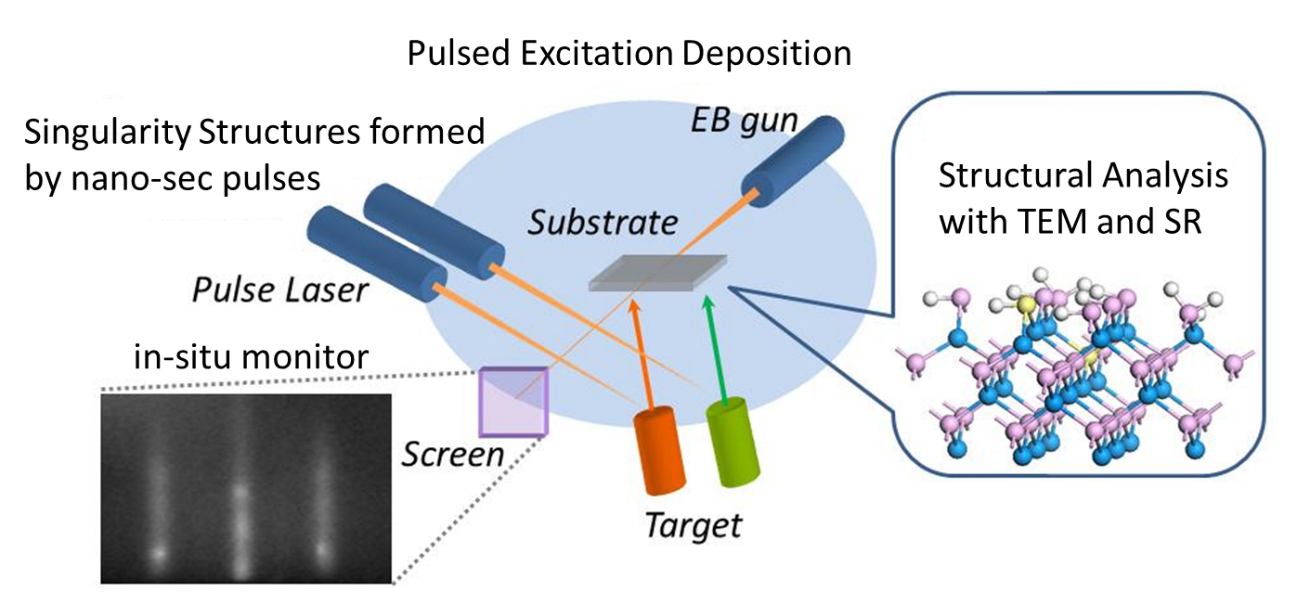
Accuracy of film composition control remains rather low at around one atomic layer (~1 second) The current accuracy of film composition control remains rather low at around one atomic layer (~1 s). This is because the supply of raw materials is conventionally controlled using mechanical apparatus such as a rotary motion shutter. We have developed a new crystal growth technique named “pulsed excitation deposition.” This uses electric pulses to control the supply sequence of the excited elements to the thin-film surface and has a precision of one 10 millionth of an atomic layer (~100 ns). Our novel method can be used to fabricate a range of singularity structures in single crystals under computer control. Based on the results of a microstructural analysis, we will attempt to improve the fabrication of singularity structures.
A01-2 Creation of singularity structure by top-down method based on equilibrium condition
- Principal Investigator / Hideto Miyake (Mie University / Professor)
- Co-Investigator / Tsutomu Araki (Ritsumeikan University / Professor)
- Co-Investigator / Reina Miyagawa (Nagoya Institute of Technology / Assistant Professor)
The technological development of the control of the generation of stress or threading dislocations will be carried out by a top-down method using singular structures under an equilibrium condition.
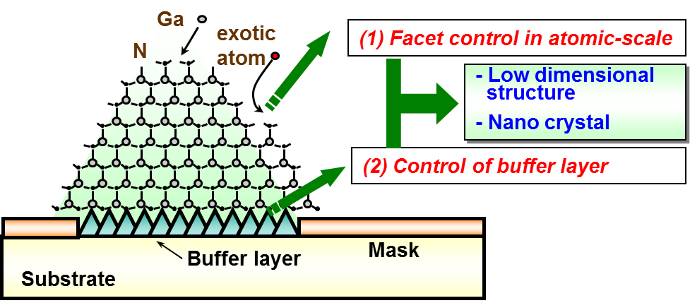
(Mie University) The effects of singularity structures, such as substrate texture, thermal annealing, and selective-area growth for the epitaxial growth of nitride semiconductors (GaN, AlN, AlGaN) will be estimated for samples fabricated by MOVPE and HVPE. Specific technologies, such as void (three-dimensional singularity structure) formation, quantum wire (one-dimensional singularity structure) fabrication and exotic atoms (zero-dimensional singularity) incorporation will be used.
(Ritsumeikan University) The control of the stress or threading dislocations by MBE with nitrogen radicals from RF plasma will be developed for forming a singularity structure at the substrate surface or in the epitaxial layer. For example, nanoscale substrate textures produced using RF plasma or a singularity interface, such as graphene, will be investigated.
(Nagoya Institute of Technology) The periodic singularity structures of the nanoscale will be formed using a femtosecond laser, and growth of the nitride semiconductors by MOVPE, HVPE, and MBE is investigated on the structures.
A01-3 Creation of a multi-dimensional and scale singularity structure in crystals and understanding of its mechanism
- Principal Investigator / Satoshi Kamiyama (Meijo University / Professor)
- Co-Investigator / Tetsuya Takeuchi (Meijo University / Professor)
- Co-Investigator / Motoaki Iwaya (Meijo University / Professor)
- Co-Investigator / Yoshio Honda (Nagoya University / Associate Professor)
In this project group, high-crystalline quality AlGaN using low-temperature deposited AlN interlayer and grooved substrate (substrate with singularity structure), high-crystalline GaInN using nano-size singularity structure, and Sb doped crystals (singularity atoms) have been realized. These intentional and control the multi-dimensional and scale singularity structure in crystals have realized the many novel devices such as world’s shortest wavelength semiconductor UV lasers, high efficiency, power UV-LEDs, and high sensitivity photosensors, and nitride-based solar cells. For further development and improvement of its novel devices, it is essential for creation of a new multi-dimensional and scale singularity structure in crystals and understanding of its mechanism.
In this project, we study the growth mechanism in the multi-dimensional and multi-scale singularity structure in crystals characterized by in situ X-ray and multi-wavelength laser beam. In addition, we invent a new singularity structure in crystal on the basis of this understanding. And, we develop the singularity structure in crystals as a new academic frontiers

A01-4 Bottom up creation of singularities by utilization of equilibrium and non-equilibrium crystal growth from vapor phase
- Principal Investigator / Yoshinao Kumagai (Tokyo University of Agriculture and Technology / Professor)
- Co-Investigator / Hisashi Murakami (Tokyo University of Agriculture and Technology / Associate Professor)
- Co-Investigator / Tomohiro Yamaguchi (Kogakuin University / Associate Professor)
- Co-Investigator / Rie Togashi (Sophia University / Assistant Professor)
- Co-Investigator / Ken Goto (Tokyo University of Agriculture and Technology / Assistant Professor)
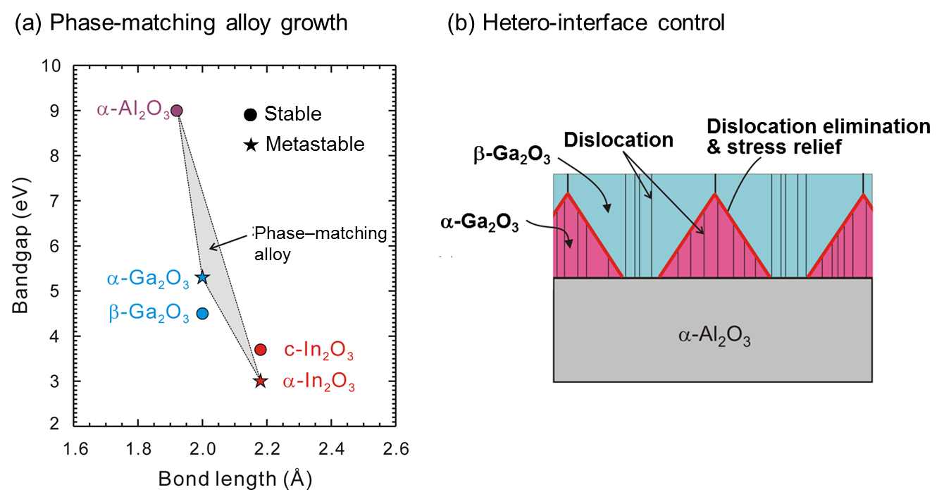
Growth of stable and metastable phases of group-III wide bandgap semiconducting sesquioxides (Al2O3, Ga2O3, and In2O3) and their alloys is investigated by halide vapor phase epitaxy (HVPE). Clarification of growth conditions for the meta-stable phase is tackled by both experimentally and theoretically, which will be important knowledge of growing phase-matching alloys having wide bandgaps of 3-9 eV. In addition, two-dimensional (2D) mixed layers of stable and metastable phases are utilized to control stresses and dislocations at the hetero-interfaces by subsequent growth under the condition suitable for stable phases. Analyses of grown layers are carried out in collaboration with groups B01 and B02, and possibility of the layers in future devices is discussed with group A02.
A01-5 Computational materials design for hetero-bond manipulation
- Principal Investigator / Tomonori Ito (Mie University / Professor)
- Co-Investigator / Toru Akiyama (Mie University / Associate Professor)
- Co-Investigator / Takahiro Kawamura (Mie University / Assistant Professor)
- Co-Investigator / Kanako Shojiki (Mie University / Assistant Professor)
- Co-Investigator / Yoshihiro Kangawa (Kyushu University / Professor)
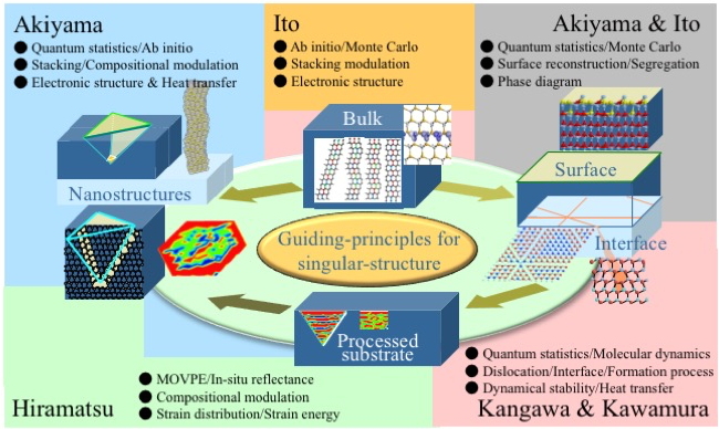
Computational materials design for manipulating hetero-bond as an element of singularity-structure (hereafter “the element”) is performed using various computational methods incorporating growth conditions. Utilizing surface (two-dimensional defect) and nanostructures with large surface area as a field of singularity-structure fabrication (hereafter “the field”), Ito and Akiyama (Mie University) investigate stacking and compositional modualtions, and structural transformation due to hetero-bonds appearing on “the field” as functions of growth conditions such as temperature and bean-equivalent pressure. Kangawa (Kyushu University) and Kawamura (Mie University) study incorporation process of hetero-bond into “the field” such as interface (two-dimensional defect) and dislocation (one-dimensional defect) to predict compositional fluctuation and segregation at and across the surface and the interface for processed substrate (three-dimensional defect). In the calculation procedure, ab initio-based approach combining pseudopoetntial and quantum statistical chemistry is mainly employed in addition to Monte Carlo and molecular dynamics methods. Moreover, collaborating with real-time strain analysis by Hiramatsu (Mie University), the interaction between “the element” and “the field” is clarified in terms of hetero-bond species to establish the guiding-principles for singularity structure fabrication.
A01-19-1 Exploration of the formation methods and control of the physical properties and functionalities of polarity-controlled nitride semiconductor singular structure
- Principal Investigator / Ryuji Katayama (Osaka University / Professor)
There is an urgent need to develop a new way of DUV light emission apart from a conventional current injection method, since the conductivity control of light emitting semiconductor materials operating at DUV regime is extremely difficult. As for the information technology field, a remarkable scale down of the system for the optical quantum computation is needed, since currently proposed system is based on the huge and unstable free space optics. So, in this work, we proceed to the further understanding and the development of the control methods for the singular structures with "polarity inversion" in the nitride semiconductors, which lead to the realization of the DUV second harmonic generation and quantum entangled photon pair generation. In addition to the exploration of the scientific knowledge on crystallography, we aim to contribute to various fields such as the industrial and medical applications, and the realization of a highly stable optical-waveguide-based quantum computer operating under the room temperature.
Page topA01-19-2 Realization of heteroepitaxial growth technology of high-quality crystals by relaxation of internal stress using self-generated voids
- Principal Investigator / Momoko Deura (The University of Tokyo / Assistant Professor)
In conventional crystal growth technologies, it is common to use high-quality substrates without any defects or surface roughness. However, in this study, we aim to realize a heteroepitaxial growth technology of high-quality crystals by relaxation of internal stress of epitaxial films using "voids", which are one of the singularity structures, just below the substrate surface. This technology will be analyzed and demonstrated by the heteroepitaxial growth of group-III nitride semiconductors on Si substrates. First, we fabricate the SiC thin films on Si substrates utilizing the surface carbonization technology and realize "SiC/Si substrates with self-generated voids and flat surface" actively using voids spontaneously generated just below the SiC thin films (i.e., the SiC/Si interface). Next, nitride semiconductor films with high crystal quality will be grown on the substrates. Finally, we will clarify the material-independent universal findings about the correlation between the internal stress and crystal quality of the epitaxial films by quantitative analyses.
Page topA01-19-3 Breaking of space inversion symmetry and creation of abnormal physical properties in asymmetrical lattices of functional oxides
- Principal Investigator / Hitoshi Tabata (The University of Tokyo / Professor)
Using various properties of functional oxides and high crystal strain tolerance due to the ionic bonding nature, we try to create new physical properties by dipole and spin fusion phenomena. Asymmetric artificial lattice is powerful technique to create novel magneto-electric dielectrics, where the crystallographic space inversion symmetry is broken by an atomic scale controlling of local crystal structure. For the garnet-type iron oxide thin film in which spin and dipole order coexist, by controlling the stacking species, period, symmetry etc., the space inversion symmetry breaking is realized. In this way, we aim to develop spin-phonon-linked magnon-induced complex physical properties by the phonon-softening: the occurrence of strong dipolar coupling and the Dzyloshinski-Moriya (DM) correlation by the synergetic effect of tilt spin and central symmetry breaking.
Page topA01-19-4 Manipulation of V-pit shape originated from dislocation and elucidation of dislocation-invalidation mechanism in GaN-based LED
- Principal Investigator / Narihito Okada (Yamaguchi University / Associate Professor)
It's interesting to note that GaN-based light emitting diodes (LED) have very high quantum efficiency despite of the high dislocation density. Superlattice (SL) is widely used to improve the LED efficiency, which has two useful effects "formation of V-pits" and "structural effect of SL". However, it is difficult to separate the two effects and their identical effects have not yet been evaluated. In this study, I propose middle-temperature-grown GaN and manipulation technique of the pit structure by introducing etching gases, which can create V-pits without the SL. It enables us to eliminate the structural effect of the SL and to evaluate only the effect of formation of the V-pits. Thus, each factor for improving LED performance will be clarified identically. Finally, I would like to optimize the V-pit shape and SL structure and contribute development of further high-efficiency LED.
Page topA01-19-5 Creation of new functionality of nitride semiconductors based on step/strain-controlled epitaxy method
- Principal Investigator / Shuhei Ichikawa (Osaka University / Assistant Professor)
Device characteristics and physical properties of III-nitride semiconductors are significantly affected by surface structures and strain during the crystal growth. Particularly for fabrication of compound semiconductors like InGaN, AlGaN, and AlInN, the composition and its distribution are changed by step-height and density of steps on growth surface. In this research, we will try to establish novel step/strain-controlled epitaxy method using in-situ doping technique of various impurities (including rare-earth ions like Eu and Tm) during metalorganic vapor phase epitaxy of nitrides. Some kind of impurities impede the diffusion of cation adatoms on growth surface, and other impurities may enhance in contrast. Thus, we expect that a growth-surface structure and strain can be flexibly controlled by selecting and doping an appropriate impurity. The new epitaxy method may realize high-density of atomic steps on vicinal (0001) growth surface without any step-bunching, and such structure, which has never been achieved, can create new functionality for nitride-semiconductor devices.
Page topA01-19-6 Theoretical analysis of GaN crystal growth by generalized ensemble method
- Principal Investigator / Masaaki Araidai (Nagoya University / Asistant Professor)
Gallium nitride (GaN) is one of the most promising semiconductor materials for next generation power devices. The crystal growth method has been intensively studied to improve the quality of GaN crystals. In the theoretical viewpoint, the statistical-mechanical calculation method coupled with the density functional theory is a powerful tool for the analysis of gas-phase and surface reactions in GaN crystal growth. The calculation method successfully gives us the energy relations between various reactions. However, it is difficult to clarify the chemical kinetics. In this study, I aim at clarifying not only the energetics but also the chemical kinetics in GaN crystal growth, using the free-energy analysis based on the generalized ensemble method. Especially, I calculate the temperature dependence of kinetic parameters, activation barrier and attempt frequency, for various processes of the gas-phase reactions and also surface adsorptions of Ga source molecules. Finally, I hope to reveal the whole picture of GaN crystal growth.
Page topA01-19-7 Development of low-temperature-growth technique for GaAs-based compound semiconductor alloys towards effective use of defects inside their crystals
- Principal Investigator / Yoriko Tominaga (Hiroshima University / Assistant Professor)
In terahertz time-domain spectroscopy (THz-TDS), photoconductive antennas (PCAs) have often used as THz emitters and detectors. This study focuses on a candidate material for PCAs which can be activated by using femtosecond fiber lasers with wavelengths of approximately 1.5 µm towards achieving less expensive and more compact THz-TDS systems. For materials which can be applied to the PCAs, they should have relatively good carrier mobility, ultrashort carrier lifetime, and large resistivity. Therefore, it is necessary to introduce some defects into the crystals and control their types and densities in order to obtain these three properties. For this purpose, I will develop low-temperature growth technique for a novel GaAs-based semiconductor alloy which may give the three properties, and reveal a relationship between growth condition and types of defects included in its crystal. Throughout a period of this study, I would like to explore a new field of defect engineering for the alloy.
Page topA01-19-8 Creation of singularity structures by molecular degrees of freedom in organic radical crystals
- Principal Investigator / Yuko Hosokoshi (Osaka Prefecture University / Professor)
Singularity structure is created on magnetic lattice and resulting quantum magnetic properties are studied. Organic radicals have highly isotropic electron spins and show remarkable quantum effect. Imperfect crystals are developed by a nonsymmetrical organic radical molecule that has molecular degrees of freedom, i.e. rotational freedom around a single bond. Disorder of molecular arrangement in crystals results in the randomness of magnetic interaction. We have developed the strategy of molecular designing in order to realize variable spin network. Based on our strategy, two-dimensional magnetic lattice is selectively synthesized and crystals with singularity structure are grown. By the crystal structural analysis and low-temperature physical measurements, singularity structures and randomness in magnetic interaction are evaluated and quantum magnetic states are examined.
Page top