B01 group
B01-1 Multiscale characterization of singularity structures and behaviors thereof
- Principal Investigator / Akira Sakai (Osaka University / Professor)
- Co-Investigator / Yasuhiko Imai (Japan Synchrotron Radiation Research Institute / Associate Senior Scientist)
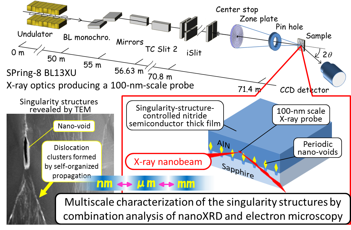
In situ Nanobeam X-ray Diffraction (nanoXRD) with 100-nm-scale spatial resolution and sub-nano-second time resolution enables a wide-range analysis of local strain and domain textures in semiconductor crystals and devices. In addition, an effective combination of nanoXRD and microscopy methods detecting microstructures and distribution of defects realizes multiscale structural characterization from nanometer to millimeter. In this project, we focus on the singularity structures and behaviors thereof mainly in nitride semiconductor crystals, such as nano-voids, dislocations,
polar/non-polar lattices influencing piezoelectric effects, etc. Being supplied with several singularity-structure-controlled materials and devices from other groups, we perform three-dimensional precise structural analysis and in situ dynamic characterization for them. By exploiting active functions of the singularity structures, we systematize extended crystallography as a new field of study and contribute to the innovation of next generation green electronics.
B01-2 Study of dynamics of carrier trapping/scattering in singularity crystal structure by means of positron annihilation
- Principal Investigator / Akira Uedono (University of Tsukuba / Professor)
- Co-Investigator / Nagayasu Oshima (National Institute of Advanced Industrial Science and Technology / Senior Researcher)
- Co-Investigator / Masatomo Sumiya (National Institute for Materials Science / Chief Researcher)
- Co-Investigator / Shoji Ishibashi (National Institute of Advanced Industrial Science and Technology / Leader, Team)
- Co-Investigator / Hironori Okumura (University of Tsukuba / Assistant Professor)
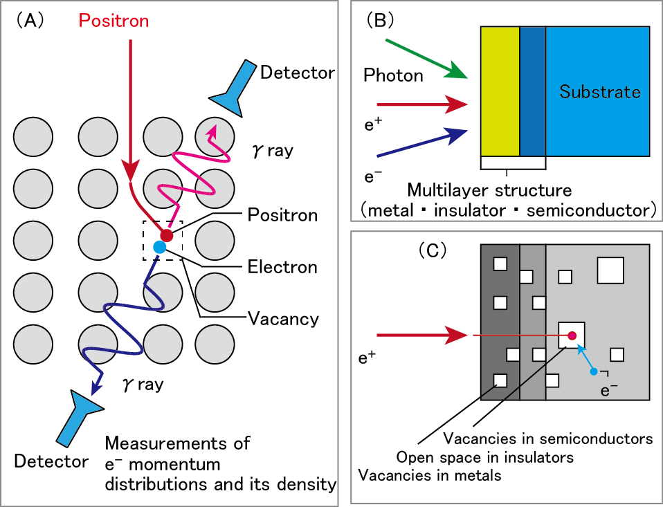
Positron annihilation is a non-destructive detection tool for vacancy-type defects or open spaces in materials (Figure A). Using this technique, one can study such singularity structures with high sensitivity, and determine their species, concentrations and depth distributions. The purpose of the present research as follows; (i) a study of carrier trapping/scattering phenomena and their optical reactions, and (ii) developments of the measurement system in order to use a positron as a probe of electric field (Figure B and C). Measurement systems equipped with positron beam, illumination system, electron beam, and bias applying electronics are installed at University of Tsukuba and National Institute of Advanced Industrial Science and Technology. We use the positron annihilation spectroscopy to study properties of the singularity structures from a view of material science, and propose guidelines for the fabrication of electric devices using such structures.
B01-3 3D spectroscopic characterization of crystal singularities and application of defects based on phonon science
- Principal Investigator / Yoshihiro Isitani (Chiba University / Professor)
- Co-Investigator / Yuzo Shinozuka (Wakayama University / Professor)
- Co-Investigator / Bei Ma (Chiba University / Research Associate)
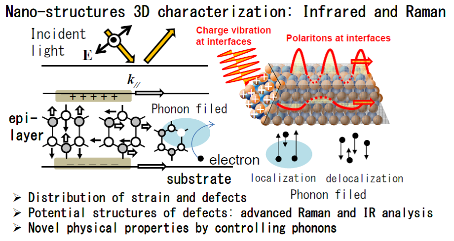
In this study, we characterize various crystal singularities and its application to the control of electronic and radiative properties of wide bandgap semiconductors by observing the interactions between carriers and phonons.
(1) Nondestructive spatially resolved characterization of crystal singularities and their physical properties
Characterization of structural properties such as strain, electronic states, and lattice vibration states in crystals of devices epitaxially grown on patterned substrates.
3D images of strain and interaction potential fields of carriers and lattice vibrations, particularly in the vicinity of dislocations and point defects
Here, we pursue the sensitive detection of fields of strain and crystal defects by the enhancement of electric field of electromagnetic waves using antenna structures, and also characterize carrier and exciton dynamics in the fields possessing crystal singularities by resonant Raman measurements using two-wavelength laser beams. Numerical analysis of the dynamics including phonon processes under nonthermal condition is also conducted. We build a bridge across the issues of defects and device properties on the basis of these studies.
(2) Application of the physics of defects to the control of optical and electrical properties for devices
We investigate the improvement of carrier transport properties, radiative efficiency, and current extraction from multi-quantum well structures by controlling the localization and delocalization of phonons using crystal singularities and the resultant increase and decrease in the interaction between phonons and carriers.
B01-19-1 Theoretical analysis of phonon behaviors at singularity structures in nitride semiconductors
- Principal Investigator / Satoshi Watanabe (The University of Tokyo / Professor)
Phonon-related properties of nitride semiconductors are important in their applications such as light emitting and power devices. However, phonon-related properties at singularity structures, for example defects, have not been well understood yet. In the present study, using machine-learning techniques, we will develop interatomic potentials that can reproduce first-principles calculation results of phonon behaviors well but need much less computational cost than the first-principles calculations, with considering the features of nitride semiconductors such as strong polarization and the existence of multiple charge states. Using the developed potentials, we will calculate phonon band structures, phonon density of states, etc. in nitride semiconductors, and clarify the change of phonon behaviors by introducing singularity structures.
Page topB01-19-2 Nondestructive characterization of crystal defects using multiphoton-excitation photoluminescence
- Principal Investigator / Tomoyuki Tanikawa (Osaka University / Associate Professor)
Novel devices based on wide band bap semiconductors, such as GaN, AlN, SiC, Ga2O3, diamond, etc., often suffer from their crystal defects. In order to realize high-performance and high-reliability devices, it is essential to discover advanced characterization technologies for crystal defects. In this study, nondestructive characterization of crystal defects in semiconductor materials using a multiphoton-excitation microscope, which is so-called "multiphoton-excitation photoluminescence", is demonstrated. Photoluminescence induced via multiphoton absorption process was corrected to detect defects inside the crystals. GaN bulk crystals or GaN homoepitaxial films are used for detailed characterization. Nonradiative characteristics of dislocations are utilized to visualize their three-dimensional structure. Based on the optical and structural properties of threading dislocations obtained by this technique, classification of crystal defects is demonstrated. To make sure the type of dislocations, the analyses using the etching pits method and a transmission electron microscope are performed. Further classification of a number of dislocations will be tried based on computing analyses. Then complicated motion of threading dislocations is investigated. Reaction of dislocations; generation of basal plane dislocations; helical motion of threading dislocations; will be characterized.
Page topB01-19-3 Effect of elastic field on local electronic and optical properties of nitride and oxide semiconductors
- Principal Investigator / Takanori Kiguchi (Tohoku University / Associate Professor)
Lattice defects and residual strain inhibits the quality of the crystal growth and the electro-optical properties of nitrides and oxides semiconductors. The target of our group is to elucidate new insights concerning the periodicity- disordered structure and electronic state such as the threading dislocation, the quantum well structure, and their elastic interactions through the local strain field in multi-scale using the electron microscopic analyses, in order to improve and create new optical and electronic devises of wide-gap and ultra-wide gap semiconductors and related materials including GaN and Ga2O3 families.
Page top